| Rule | Description | Lambda | ||
|---|---|---|---|---|
| SCMOS | SUBM | DEEP | ||
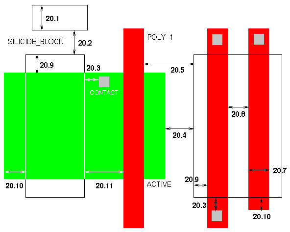
| 20.1 | Minimum SB width | 4 | 4 | 4 |
| 20.2 | Minimum SB spacing | 4 | 4 | 4 |
| 20.3 |
Minimum spacing, SB to contact
(no contacts allowed inside SB) |
2 | 2 | 2 |
| 20.4 | Minimum spacing, SB to external active | 2 | 2 | 2 |
| 20.5 | Minimum spacing, SB to external poly | 2 | 2 | 2 |
| 20.6 |
Resistor is poly inside SB; poly ends stick out for contacts
the entire resistor must be outside well and over field |
|||
| 20.7 | Minimum poly width in resistor | 5 | 5 | 5 |
| 20.8 |
Minimum spacing of poly resistors
(in a single SB region) |
7 | 7 | 7 |
| 20.9 | Minimum SB overlap of poly or active | 2 | 2 | 2 |
| 20.10 | Minimum poly or active overlap of SB | 3 | 3 | 3 |
| 20.11 |
Minimum spacing, SB to poly
(in a single active region) |
3 | 5 | 5 |
NOTE: Some processes do not support both silicide block over active and silicide block over poly. Refer to the individual process description pages.