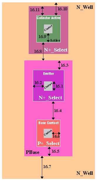
The pbase layer is an active area that is implanted with the pbase implant to form the base of the NPN bipolar transistor. The base contact is enclosed in p-select. The emitter is an n-select region within (and on top of) the base. The entire pbase sits in an n-well that is the collector. The collector contact is a well contact, but the overlaps are larger. Active should not be used inside of pbase.
| Rule | Description | Lambda | ||
|---|---|---|---|---|
| SCMOS | SUBM | DEEP | ||
| 16.1 | All active contact | 2 x 2 | n/a | n/a |
| 16.2 | Minimum emitter select overlap of contact | 3 | n/a | n/a |
| 16.3 | Minimum pbase overlap of emitter select | 2 | n/a | n/a |
| 16.4 |
Minimum spacing between emitter select
and base select |
4 | n/a | n/a |
| 16.5 | Minimum pbase overlap of base select | 2 | n/a | n/a |
| 16.6 | Minimum base select overlap of contact | 2 | n/a | n/a |
| 16.7 | Minimum nwell overlap of pbase | 6 | n/a | n/a |
| 16.8 | Minimum spacing between pbase and collector active | 4 | n/a | n/a |
| 16.9 | Minimum collector active overlap of contact | 2 | n/a | n/a |
| 16.10 | Minimum nwell overlap of collector active | 3 | n/a | n/a |
| 16.11 | Minimum select overlap of collector active | 2 | n/a | n/a |