The DEEP_N_WELL layer provides access to the DNW layer in the TSMC 0.18 and 0.25 processes. This provides a layering sometimes called "triple-well" in which an n-well sits in the p-substrate, and then a p-well sits fully inside of the n-well; it is then possible to construct NMOS devices inside of that isolated p-well. The isolated p-well is surrounded by a fence of standard N_WELL (around its periphery), and by DEEP_N_WELL underneath. The N_WELL fence makes direct electrical contact with the DEEP_N_WELL plate beneath it.
DEEP_N_WELL is available in technology codes SCN5M_SUBM, SCN5M_DEEP, SCN6M_SUBM and SCN6M_DEEP but only where these are to be fabricated on TSMC foundry runs. To gain a better understanding of this layer, the TSMC vendor-rule design rule documentation should be studied.
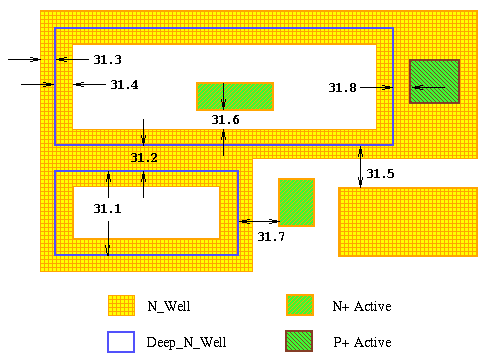
| Rule | Description | Lambda | ||
| SCMOS | SUBM | DEEP | ||
| 31.1 | Minimum Width, Deep_N_Well | n/a | 30 | 34 |
| 31.2 | Minimum Spacing, Deep_N_Well to Deep_N_Well | n/a | 50 | 56 |
| 31.3 | Minimum extension, N_Well beyond Deep_N_Well edge | n/a | 15 | 17 |
| 31.4 | Minimum overlap, N_Well over Deep_N_Well edge | n/a | 20 | 23 |
| 31.5 | Minimum spacing, Deep_N_Well to unrelated N_Well | n/a | 35 | 39 |
| 31.6 | Minimum spacing, N+Active in isolated P-well, to N_Well | n/a | 5 | 6 |
| 31.7 | Minimum spacing, external N+Active to Deep_N_Well | n/a | 30 | 34 |
| 31.8 | Minimum spacing, P+Active in N_Well to its Deep_N_Well | n/a | 10 | 13 |